- 您现在的位置:买卖IC网 > Sheet目录369 > W971GG6JB25I (Winbond Electronics)IC DDR2 SDRAM 1GBIT 84WBGA
�� �
�
�W971GG6JB�
�Notes:�
�1.� To� guarantee� ODT� off,� V� REF� must� be� valid� and� a� LOW� level� must� be� applied� to� the� ODT� pin.�
�2.� V� REF� must� be� within� ±� 300� mV� with� respect� to� V� DDQ� /2� during� supply� ramp� time.�
�3.� V� DD� /V� DDL� voltage� ramp� time� must� be� no� greater� than� 200� mS� from� when� V� DD� ramps� from� 300� mV� to� V� DD� min.�
�4.� The� V� DDQ� voltage� ramp� time� from� when� V� DD� min� is� achieved� on� V� DD� to� when� V� DDQ� min� is� achieved� on� V� DDQ� must� be� no�
�greater� than� 500� mS.�
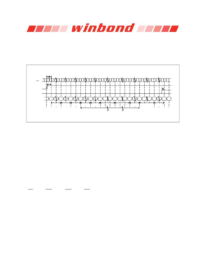
�t� CH� t� CL�
�CLK�
�CLK�
�CKE�
�ODT�
�t� IS�
�t� IS�
�Command�
�NOP�
�400nS�
�PRE�
�ALL�
�t� RP�
�EMRS�
�t� MRD�
�MRS�
�t� MRD�
�PRE�
�ALL�
�t� RP�
�REF�
�t� RFC�
�REF�
�t� RFC�
�MRS�
�t� MRD�
�EMRS�
�Follow� OCD�
�EMRS�
�t� OIT�
�ANY�
�CMD�
�Flow� chart�
�DLL�
�Enable�
�DLL�
�Reset�
�min� 200� Cycle�
�OCD�
�Default�
�OCD�
�CAL.� Mode�
�Exit�
�Figure� 1� –� Initialization� sequence� after� power-up�
�8.2�
�Mode� Register� and� Extended� Mode� Registers� Operation�
�For� application� flexibility,� burst� length,� burst� type,� CAS� Latency,� DLL� reset� function,� write� recovery�
�time� (WR)� are� user� defined� variables� and� must� be� programmed� with� a� Mode� Register� Set� (MRS)�
�command.� Additionally,� DLL� disable� function,� driver� impedance,� additive� CAS� Latency,� ODT� (On� Die�
�Termination),� single-ended� strobe� and� OCD� (off� chip� driver� impedance� adjustment)� are� also� user�
�defined� variables� and� must� be� programmed� with� an� Extended� Mode� Register� Set� (EMRS)� command.�
�Contents� of� the� Mode� Register� (MR)� or� Extended� Mode� Registers� EMR� (1),� EMR� (2)� and� EMR� (3)� can�
�be� altered� by� re-executing� the� MRS� or� EMRS� Commands.� Even� if� the� user� chooses� to� modify� only� a�
�subset� of� the� MR� or� EMR� (1),� EMR� (2)� and� EMR� (3)� variables,� all� variables� within� the� addressed�
�register� must� be� redefined� when� the� MRS� or� EMRS� commands� are� issued.�
�MRS,� EMRS� and� Reset� DLL� do� not� affect� array� contents,� which� mean� re-initialization� including� those�
�can� be� executed� at� any� time� after� power-up� without� affecting� array� contents.�
�8.2.1�
�Mode� Register� Set� Command� (MRS)�
�(� CS� =� "L",� RAS� =� "L",� CAS� =� "L",� WE� =� "L",� BA0� =� "L",� BA1� =� "L",� BA2� =� "L",� A0� to� A12� =�
�Register� Data)�
�The� mode� register� stores� the� data� for� controlling� the� various� operating� modes� of� DDR2� SDRAM.� It�
�programs� CAS� Latency,� burst� length,� burst� sequence,� test� mode,� DLL� reset,� Write� Recovery� (WR)� and�
�various� vendor� specific� options� to� make� DDR2� SDRAM� useful� for� various� applications.� The� default�
�value� in� the� Mode� Register� after� power-up� is� not� defined,� therefore� the� Mode� Register� must� be�
�programmed� during� initialization� for� proper� operation.�
�The� DDR2� SDRAM� should� be� in� all� bank� precharge� state� with� CKE� already� HIGH� prior� to� writing� into�
�the� mode� register.� The� mode� register� set� command� cycle� time� (t� MRD� )� is� required� to� complete� the� write�
�operation� to� the� mode� register.� The� mode� register� contents� can� be� changed� using� the� same� command�
�and� clock� cycle� requirements� during� normal� operation� as� long� as� all� banks� are� in� the� precharge� state.�
�The� mode� register� is� divided� into� various� fields� depending� on� functionality.� Burst� length� is� defined� by�
�Publication� Release� Date:� Sep.� 24,� 2013�
�-� 10� -�
�Revision� A09�
�发布紧急采购,3分钟左右您将得到回复。
相关PDF资料
W971GG8JB-25
IC DDR2 SDRAM 1GBIT 60WBGA
W9725G6IB-25
IC DDR2-800 SDRAM 256MB 84-WBGA
W9725G6JB25I
IC DDR2 SDRAM 256MBIT 84WBGA
W9725G6KB-25I
IC DDR2 SDRAM 256MBIT 84WBGA
W972GG6JB-3I
IC DDR2 SDRAM 2GBITS 84WBGA
W9751G6IB-25
IC DDR2-800 SDRAM 512MB 84-WBGA
W9751G6KB-25
IC DDR2 SDRAM 512MBIT 84WBGA
W9812G6JH-6I
IC SDRAM 128MBIT 54TSOPII
相关代理商/技术参数
W971GG6JB-25I
制造商:Winbond Electronics 功能描述:-40~85 1GB DDR2 FOR INDUSTRY
W971GG6JB25ITR
制造商:Winbond Electronics Corp 功能描述:1G, DDR2-800, X16, IND TEMP
W971GG6JB25TR
制造商:Winbond Electronics Corp 功能描述:NR, DDR2-800, X16
W971GG6JB-3
制造商:Winbond Electronics Corp 功能描述:1GBIT DDRII
W971GG6KB-18
制造商:Winbond Electronics Corp 功能描述:1G, DDR2-1066, X16 制造商:Winbond Electronics Corp 功能描述:IC MEMORY
W971GG8JB
制造商:WINBOND 制造商全称:Winbond 功能描述:16M × 8 BANKS × 8 BIT DDR2 SDRAM
W971GG8JB-25
功能描述:IC DDR2 SDRAM 1GBIT 60WBGA RoHS:是 类别:集成电路 (IC) >> 存储器 系列:- 标准包装:72 系列:- 格式 - 存储器:RAM 存储器类型:SRAM - 同步 存储容量:4.5M(256K x 18) 速度:133MHz 接口:并联 电源电压:3.135 V ~ 3.465 V 工作温度:0°C ~ 70°C 封装/外壳:100-LQFP 供应商设备封装:100-TQFP(14x20) 包装:托盘
W9725G6IB-25
功能描述:IC DDR2-800 SDRAM 256MB 84-WBGA RoHS:是 类别:集成电路 (IC) >> 存储器 系列:- 标准包装:1,000 系列:- 格式 - 存储器:EEPROMs - 串行 存储器类型:EEPROM 存储容量:4K (512 x 8) 速度:400kHz 接口:I²C,2 线串口 电源电压:2.7 V ~ 5.5 V 工作温度:-40°C ~ 85°C 封装/外壳:8-SOIC(0.173",4.40mm 宽) 供应商设备封装:8-MFP 包装:带卷 (TR)